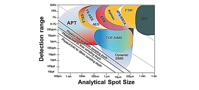
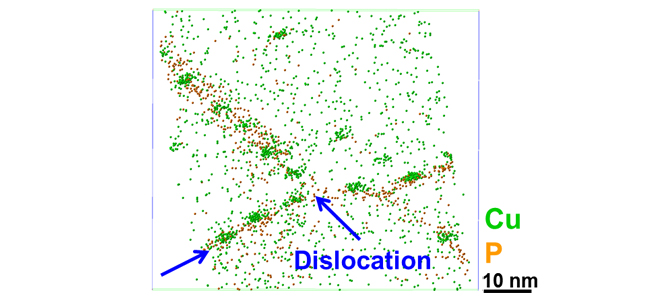
 Atom Probe Tomography (APT or 3D Atom Probe) is the only material analysis technique offering extensive capabilities for both 3D imaging and chemical composition measurements at the atomic scale (around 0.1-0.3nm resolution in depth and 0.3-0.5nm laterally). Since its early developments, Atom Probe Tomography has contributed to major advances in materials science.
The sample is prepared in the form of a very sharp tip. The cooled tip is biased at high DC voltage (3-15 kV). The very small radius of the tip and the High Voltage induce a very high electrostatic field (tens V/nm) at the tip surface, just below the point of atom evaporation. Under laser or HV pulsing, one or more atoms are evaporated from the surface, by field effect (near 100% ionization), and projected onto a Position Sensitive Detector (PSD) with a very high detection efficiency. Ion efficiencies are as high as 80%, the highest analytical efficiency of any 3D microscopy.


